AMD today charted out its plans for the next few years of product development, with an array of new CPUs and GPUs in the development pipeline.
On the GPU front are two new datacenter-oriented GPUs...
On the CPU side of things, AMD talked extensively about the forthcoming Zen 2 architecture. The goal of the original Zen architecture was to get AMD, at the very least, competitive with what Intel had to offer. AMD knew that Zen would not take the performance lead from Intel, but the pricing and features of its chips made them nonetheless attractive, especially in workloads that highlighted certain shortcomings of Intel's parts (fewer memory channels, less I/O bandwidth). Zen 2 promises to be not merely competitive with Intel, but superior to it.
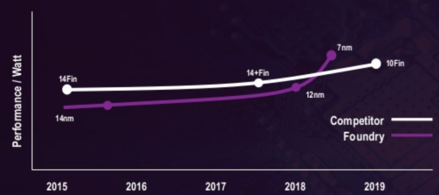
Enlarge / TSMC's 7nm process gives AMD the manufacturing advantage over Intel.
AMD
Key to this is TSMC's 7nm process, which offers twice the transistor density of the 14nm process the original Zen parts used. For the same performance level, power is reduced by about 50 percent, or, conversely, at the same power consumption, performance is increased by about 25 percent. TSMC's 14nm and 12nm processes both trail behind Intel's 14nm process in terms of performance per watt, but with 7nm, TSMC will take the lead.
Zen 2 will also address certain weak aspects of the original Zen. For example, the original Zen used 128-bit data paths to handle 256-bit AVX2 operations; each operation was split into two parts and processed sequentially. In workloads using AVX2, this gave Intel, with its native 256-bit implementation, a huge advantage. Zen 2 doubles the floating-point execution units and data paths to be 256-bit, doubling the bandwidth available and greatly improving the performance of this code. For integer workloads, branch prediction and prefetching have been made more accurate and some caches enlarged.
Zen 2 will also offer improved hardware protection against some variants of the Spectre attacks.
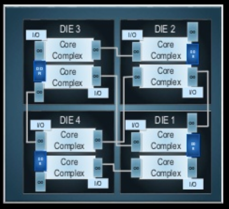
The original Zen used a multichip module design. Chips used one, two, or four dies (for Ryzen, first-generation Threadripper, and Epyc/second-generation Threadripper, respectively) all put together into a single package. Each die had two Core Complexes (blocks of four cores), two memory controllers, some Infinity Fabric links (for connections between dies), and some PCIe channels. This made it straightforward for AMD to scale from the single-die, 8-core/16-thread Ryzen up to the 32-core/64-thread Epyc.
The original Zen topology: each die has all the parts needed for a complete processor.
AMD
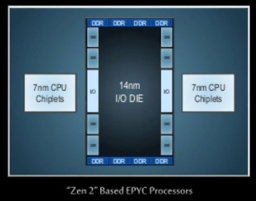
Zen 2 is taking a very different approach, albeit one that still uses a multichip design. Instead of having each die contain CPUs, memory controllers, and I/O, the new design splits up the different roles. There will be a single 14nm I/O die, with eight memory controllers, eight Infinity Fabric ports, and PCIe lanes, and then a number of 7nm "chiplets" containing only CPUs and Infinity Fabric. This new approach should remedy some of the more awkward aspects of the original Zen; for example, there is a significant latency overhead when a core on one Zen die has to use memory from another die. With the Zen 2 design, memory latency should become much more uniform.
The new Zen 2 design: common I/O functions are put on the 14nm I/O die, with the 7nm "chiplets" containing only CPUs.
AMD
AMD says that Zen 2 is sampling now, with processors due to hit the market in 2019. Zen 3, using an enhanced version of the 7nm process, is currently "on track" and likely to land in 2020, and Zen 4, on a more advanced process, is currently in the design stage.


 #sarcasm